China's chipmakers pay higher prices to bypass EUV restrictions
DUV workarounds force Chinese foundries to accept lower yields and larger dies as they chase advanced nodes without ASML's latest tools.
By Lorenzo Patterson ·
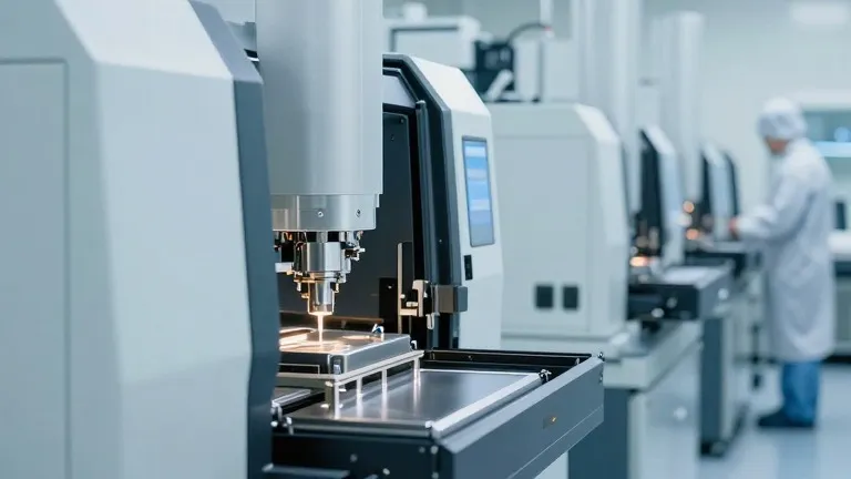
Chinese chipmakers can produce advanced processors without extreme ultraviolet lithography machines, but the method raises manufacturing costs and lowers output efficiency. Export controls have kept ASML's EUV tools out of the country, forcing domestic firms to rely on older deep ultraviolet equipment. This reliance requires multiple exposure steps to print critical layers, a process that increases the chance of defects and extends production time.
The financial impact is measurable. Industry expert Chris Mack notes that three exposures on a 193 immersion tool cost roughly the same as one EUV exposure. When manufacturers require four masks, EUV becomes the cheaper option. Despite this, Chinese foundries continue to use the multi-patterning method to bridge the technology gap. Morgan Stanley estimates that Chinese DRAM maker CXMT currently produces only one-third as many bits per wafer as Western competitors. The bank identifies lithography access as a hard ceiling for Chinese memory development.
SMIC has demonstrated the technical viability of this approach. A 2023 teardown of the Huawei Mate 60 Pro revealed that its Kirin 9000S processor was fabricated using a 7nm-class process without EUV. Recent analysis of the Kirin 9030 suggests SMIC has pushed its DUV-based process closer to 5nm density levels. While this progress narrows the gap, it still trails the leading processes from TSMC and Samsung. Mack argues that node labels like 5nm have little meaning without context, and SMIC's N+3 process remains less scaled than established 5nm nodes.
The physical constraints of DUV patterning create specific engineering challenges. Each additional pattern must align precisely with previous layers, leading to accumulated overlay errors. Designers often add extra space around features to compensate, which enlarges the chip die. Since wafers cost tens of thousands of dollars, reducing the number of dies per wafer is expensive. Mack summarizes the economic reality: You don't sell wafers, you sell die.
DUV technology still has room for advancement. Micron developed its 1-alpha DRAM without EUV, using tight process control and multiple patterning. Mack states that Micron pushed 193nm technology farther than other memory makers. Morgan Stanley believes CXMT's planned move to 1-alpha DRAM for HBM3e is achievable without EUV. Douglas Fuller, a researcher at Copenhagen Business School, expects advanced packaging to allow firms to use DUV for the latest DRAM generations by the end of the decade.
However, the efficiency gap persists at the most advanced nodes. Micron eventually adopted EUV for its 1-gamma DRAM, claiming more than 30% greater bit density per wafer than the previous generation. EUV has its own issues, such as stochastic effects, but Mack says he would be hard pressed to believe a 3nm or 2nm node is economically viable without it. Chinese firms can continue to push DUV limits by accepting larger dies, poorer yields, or longer manufacturing times.
Morgan Stanley projects that CXMT will remain on 1-alpha DRAM without EUV but will increase its share of global DRAM bit supply from 14% in 2026 to 16% in 2028. This growth is expected to come from new greenfield capacity rather than higher yields per wafer. The bank also forecasts that China's AI chip self-sufficiency will rise from 42% in 2025 to 70% by 2030, even as gaps in EUV access and advanced software remain.
The strategy involves trading cost for capability. By using multiple DUV exposures, Chinese manufacturers keep production moving despite equipment restrictions. The approach allows them to maintain domestic output levels while absorbing the higher costs associated with complex patterning. As the industry moves toward more advanced nodes, the efficiency difference between DUV and EUV processes will likely widen, forcing further trade-offs in design and manufacturing.
Source: Tom's Hardware